Special Function Register(SFR) in 8051 Microcontroller
8051 Microcontroller Data Processing
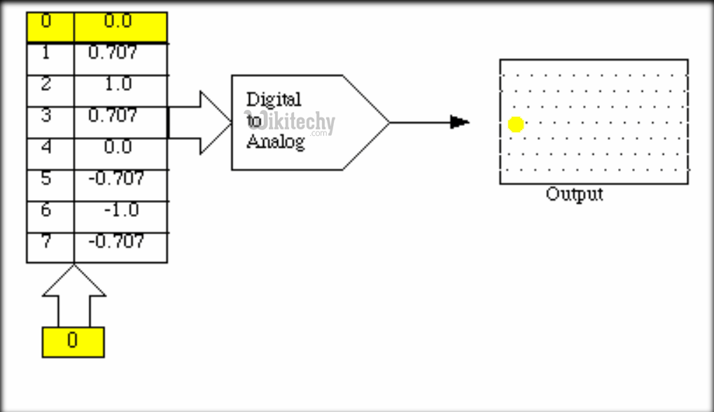
- This microcontroller is used to process the data effectively and it's used in special functions like Converting your digital data into analog value.
8051 Microcontroller Data Processing
Serial and Parallel Data Processing
- A processing in which one task is completed at a time and all the tasks are run by the processor in a sequence.

Serial Data Processing
- A type of processing in which multiple tasks are completed at a time by different processors
Parallel Data Processing
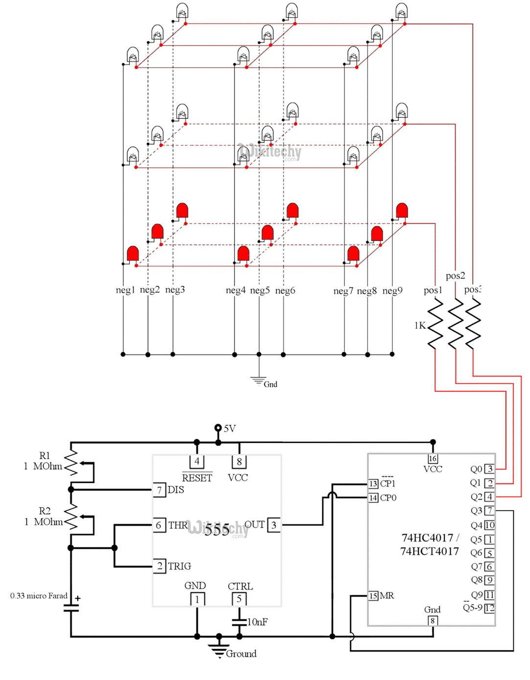
Timer Control Circuit
- The 8051 has two counters/timers which can be used either as timer to generate a time delay or as counter to count events happening outside the microcontroller.
Timer Control Circuit
Data Processing Circuit
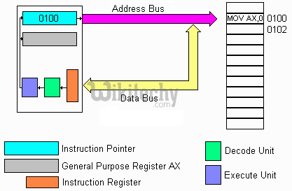
- The data bus carries the data, while address bus carries the location of the data.
- Address Bus -
- It is a group of lines(wires) used to refer a physical location in memory.
- The number of lines in address bus determines the number of physical memory locations.
- It is unidirectional.
- 8085 has 16-bit address bus.
- Data Bus -
- It is also called memory bus
- It is used to carry the data and it is bidirectional
- The width of the data bus is determined by the size of the individual memory blocks(in 8085, it is 8-bit)
Data Processing Circuit
8051 Microcontroller Architecture
The Following diagram shows the 8051 microcontroller Architecture
8051 Microcontroller Architecture
Internal Architecture of 8051 Microcontroller
Here we have seen the internal architecture of the 8051 Microcontroller
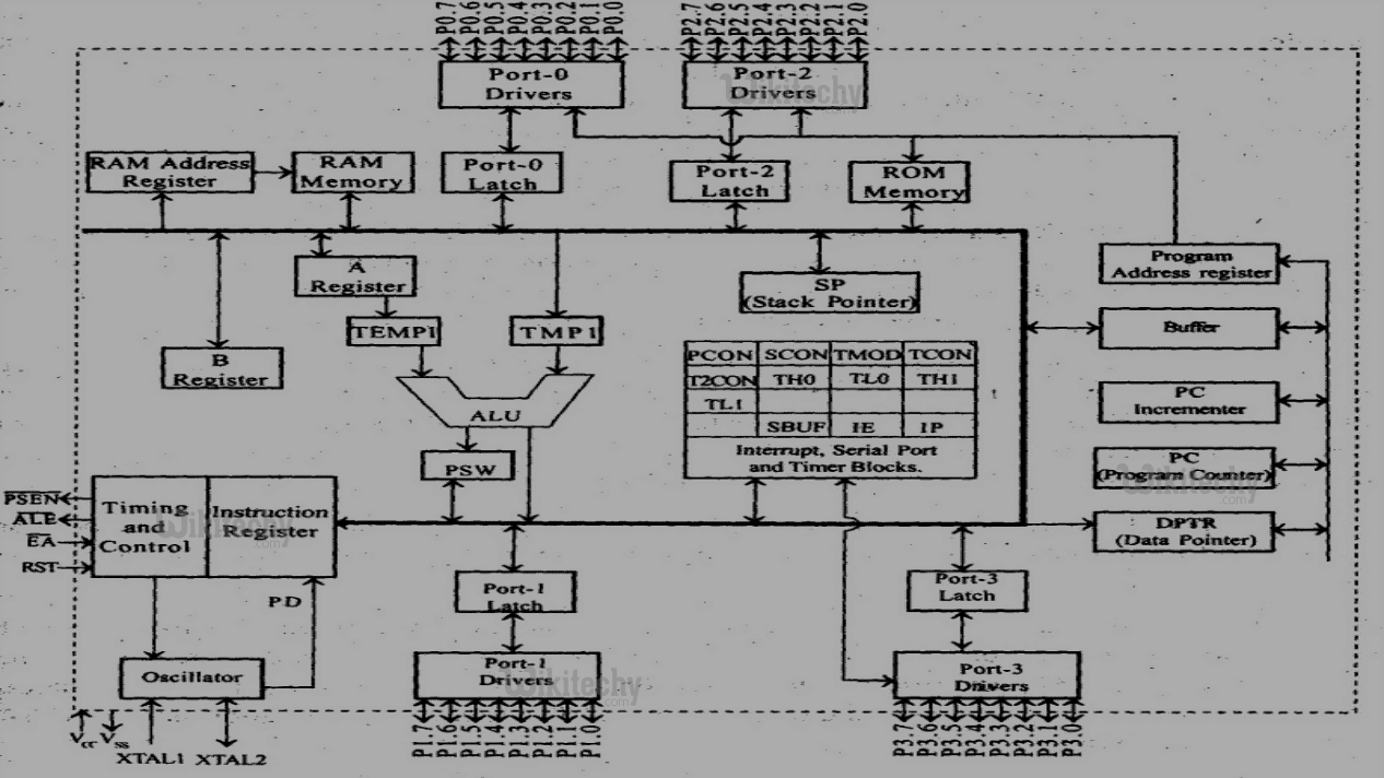
Internal Architecture of 8051 Microcontroller
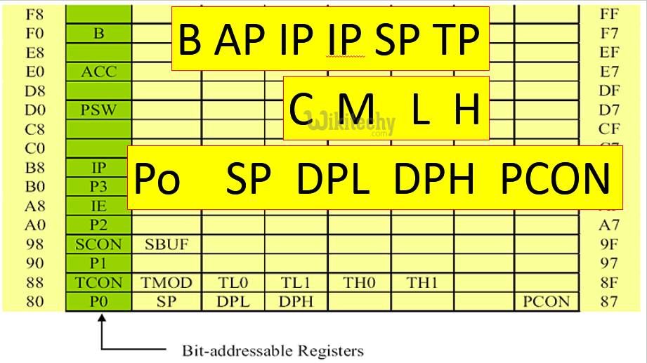
Special Function Register(SFR) in 8051 Microcontroller
Special Function Register(SFR) in 8051 Microcontroller
List of 8051 Microcontroller Special Function Registers
- Math or CPU Registers: A and B
- Status Register: PSW (Program Status Word)
- Pointer Registers: DPTR (Data Pointer – DPL, DPH) and SP (Stack Pointer)
- I/O Port Latches: P0 (Port 0), P1 (Port 1), P2 (Port 2) and P3 (Port 3)
- Peripheral Control Registers: PCON, SCON, TCON, TMOD, IE and IP
- Peripheral Data Registers: TL0, TH0, TL1, TH1 and SBUF
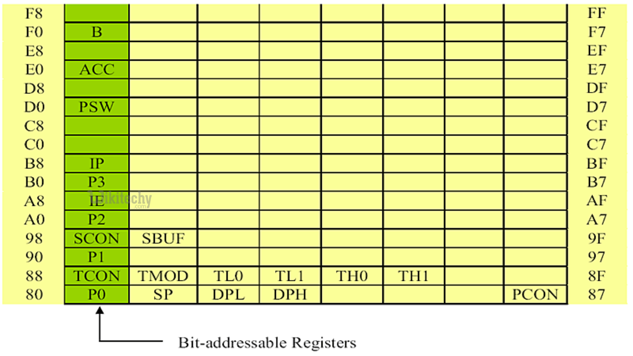
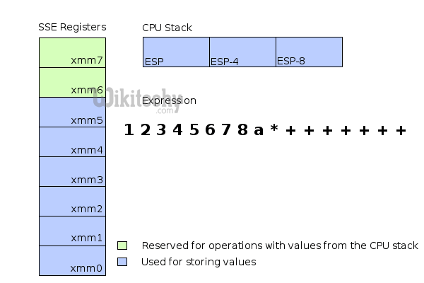
Bit Addressable Register
Short cut to memorize the SFR in microcontroller :
Short cut to memorize the SFR in microcontroller
Math or CPU Registers: A or Accumulator (ACC)
- The Accumulator or Register A is the most important and most used
- Register A is located => At address E0H
- Accumulator is used to hold the data for almost all the ALU Operations.
- Some of the operations are:
- Arithmetic Operations like Addition, Subtraction, Multiplication etc.
- Logical Operations like AND, OR, NOT etc.
- Data Transfer Operations (between 8051 and External Memory).
- The name “Accumulator” came from the fact that, this register is used to accumulate (or store) the result of all Arithmetic and most of the Logical Operations.
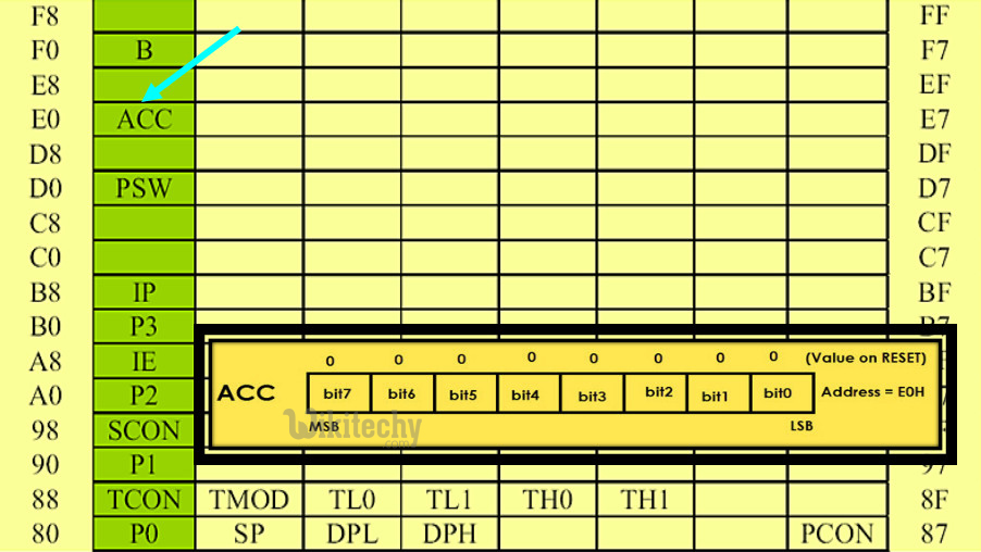
Accumulator
Functions of Accumulator
Math or CPU Registers: B (Register B)
- The B Register is used along with the ACC in Multiplication and Division operations. These two operations are performed on data that are stored only in Registers A and B.
- During Multiplication Operation, one of the operand (multiplier or multiplicand) is stores in B Register and also the higher byte of the result.
- In case of Division Operation, the B Register holds the divisor and also the remainder of the result. It can also be used as a General Purpose Register for normal operations and is often used as an Auxiliary Register by Programmers to store temporary results.
- Register B is located at the address F0H of the SFR Address Space.
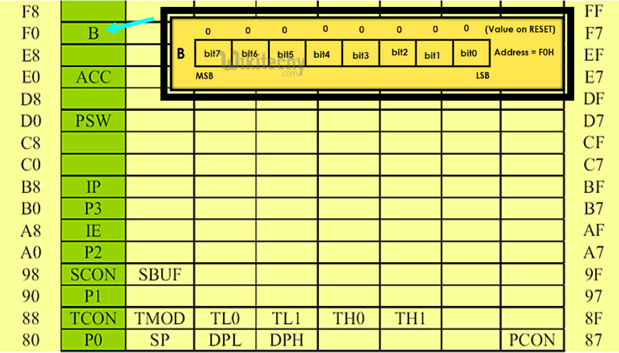
Register B in 8051 Microcontroller SFR
B Register in 8085 Microcontroller
Program Status Word (PSW)
- The PSW or Program Status Word Register is also called as Flag Register and is one of the important SFRs.
- The PSW Register consists of Flag Bits, which help the programmer in checking the condition of the result and also make decisions.
- Flags are 1-bit storage elements that store and indicate the nature of the result that is generated by execution of certain instructions.
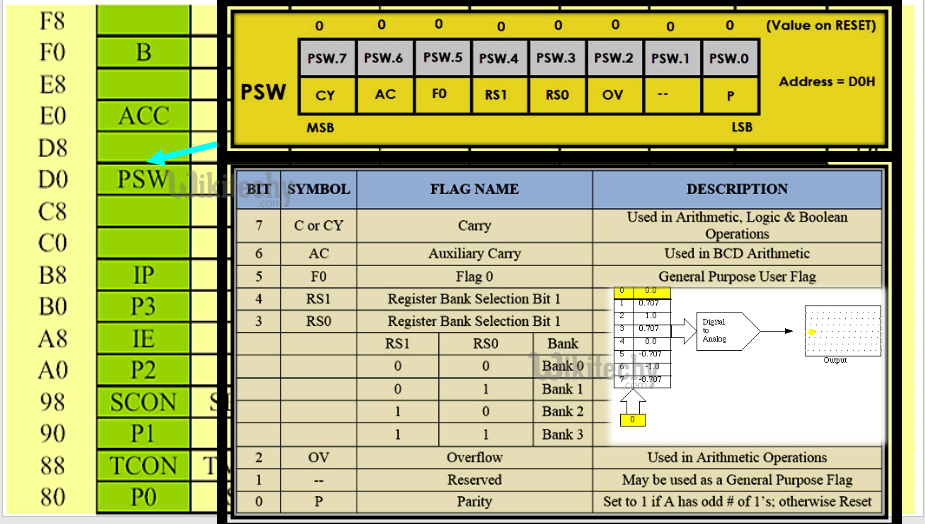
Program status word Register
Working of Program Status Word (PSW) in 8051 Microcontroller
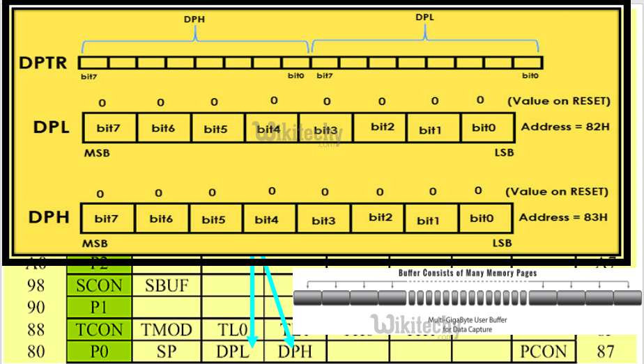
Pointer Registers - Data Pointer (DPTR – DPL and DPH)
- The Data Pointer is a 16-bit Register and is physically the combination of DPL (Data Pointer Low) and DPH (Data Pointer High) SFRs. The Data Pointer can be used as a single 16-bit register (as DPTR) or two 8-bit registers (as DPL and DPH).
- DPTR doesn’t have a physical Memory Address but the DPL (Lower Byte of DPTR) and DPH (Higher Byte of DPTR) have separate addresses in the SFR Memory Space. DPL = 82H and DPH = 83H.
- The DPTR Register is used by the programmer addressing external memory (Program – ROM or Data – RAM).
Pointer Registers - Data Pointer (DPTR – DPL and DPH)
8051 Microcontroller Data Pointer Register
Pointer Registers - Stack Pointer (SP)
- SP or Stack Pointer points out to the top of the Stack and it indicates the next data to be accessed. Stack Pointer can be accesses using PUSH, POP, CALL and RET Instructions. The Stack Pointer is an 8-bit register and upon reset, the Stack Pointer is initialized with 07H.
- When writing a new data byte into the stack, the SP (Stack Pointer) is automatically incremented by 1 and the new data is written at an address SP+1. When reading data from stack, the data is retrieved from the Address in SP and after that the SP is decremented by 1 (SP-1).
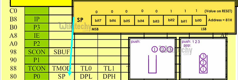
Pointer Registers - Stack Pointer (SP) in 8051 Microcontroller
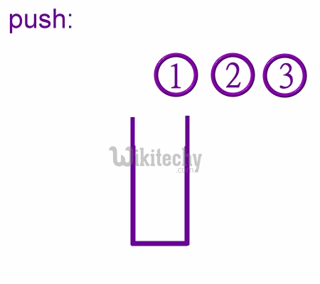
Push Operations - Stack Pointer (SP)
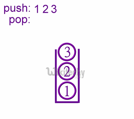
Pop Operations- Stack Pointer (SP)
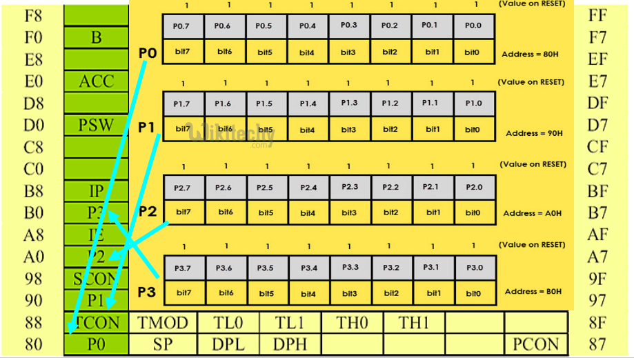
Pointer Registers - I/O Port Registers (P0, P1, P2 and P3)
- The 8051 Microcontroller four Ports which can be used as Input and/or Output. These four ports are P0, P1, P2 and P3. Each Port has a corresponding register with same names (the Port Registers are also P0, P1, P2 and P3). The addresses of the Port Registers are as follows: P0 – 80H, P1 – 90H, P2 – A0H and P2 – B0H.
- Each bit in these SFRs corresponds to one physical Pin in the 8051 Microcontroller. All these Port Registers are both Bit Addressable and Byte Addressable. Writing 1 or 0 on a Port Register Bit will reflect as an appropriate voltage (5V and 0V) on the corresponding Pin.
- If a Port Bit is SET (declared as 1), the corresponding Port Pin will be configured as Input and similarly if a Port Bit is CLEARED (declared as 0), the corresponding Port Pin is configured as Output. Upon reset, all the Port Bits are SET (1) and hence, all the Port Pins are configured as Inputs.
Pointer Registers - I/O Port Registers (P0, P1, P2 and P3)
Pointer Registers in Real world
Peripheral Control Registers - PCON (Power Control)
- The PCON or Power Control register, as the name suggests is used to control the 8051 Microcontroller’s Power Modes and is located at 87H of the SFR Memory Space. Using two bits in the PCON Register, the microcontroller can be set to Idle Mode and Power Down Mode.
- During Idle Mode, the Microcontroller will stop the Clock Signal to the ALU (CPU) but it is given to other peripherals like Timer, Serial, Interrupts, etc. In order to terminate the Idle Mode, you have to use an Interrupt or Hardware Reset.
- In the Power Down Mode, the oscillator will be stopped and the power will be reduced to 2V. To terminate the Power Down Mode, you have to use the Hardware Reset.
- Apart from these two, the PCON Register can also be used for few additional purposes. The SMOD Bit in the PCON Register is used to control the Baud Rate of the Serial Port.
- There are two general purpose Flag Bits in the PCON Register, which can be used by the programmer during execution.
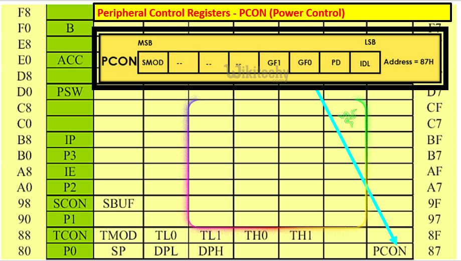
Peripheral Control Registers - PCON (Power Control) in 8051 microcontroller
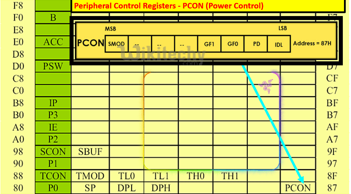
Peripheral Control Registers - PCON (Power Control) in Real World
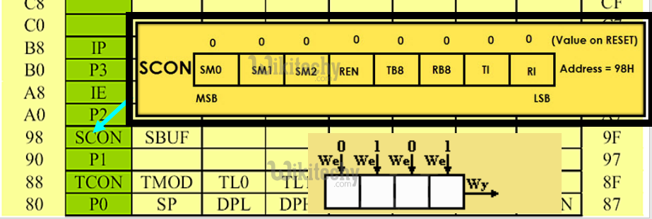
Peripheral Control Registers - SCON (Serial Control)
- The Serial Control or SCON SFR is used to control the 8051 Microcontroller’s Serial Port. It is located as an address of 98H. Using SCON, you can control the Operation Modes of the Serial Port, Baud Rate of the Serial Port and Send or Receive Data using Serial Port.
- SCON Register also consists of bits that are automatically SET when a byte of data is transmitted or received.
Peripheral Control Registers - SCON (Serial Control) of 8051 Microcontroller
Serial data processing in peripheral Control Registers - SCON (Serial Control)
Peripheral Control Registers - SCON (Serial Control) - Serial Port Mode Control Bits
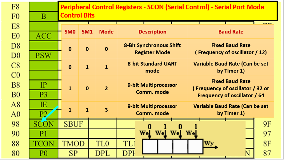
SCON (Serial Control) - Serial Port Mode Control Bits in 8051 Microcontroller
Peripheral Control Registers - TCON (Timer Control)
- Timer Control or TCON Register is used to start or stop the Timers of 8051 Microcontroller. It also contains bits to indicate if the Timers has overflowed. The TCON SFR also consists of Interrupt related bits.
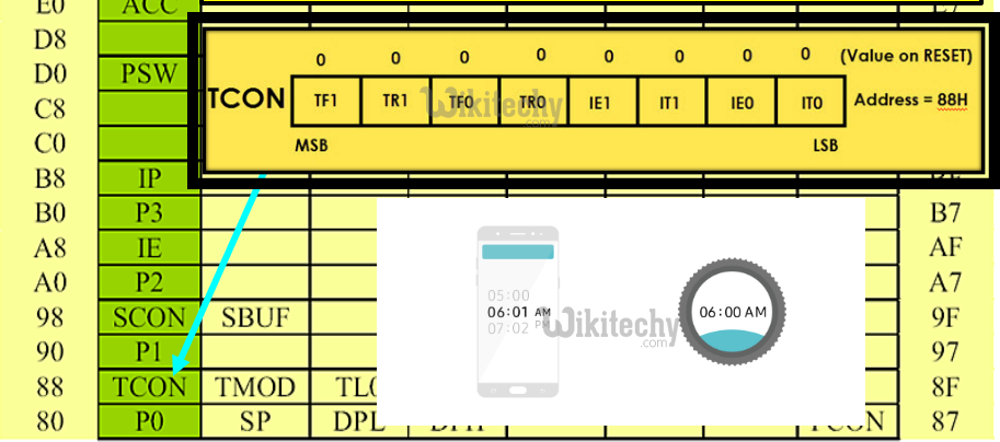
TCON (Timer Control) in 8051 Microcontroller

Peripheral Control Registers - TCON (Timer Control) in Real world
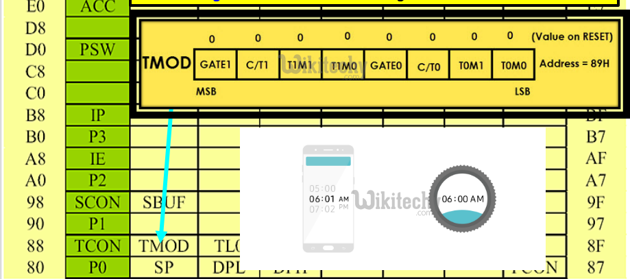
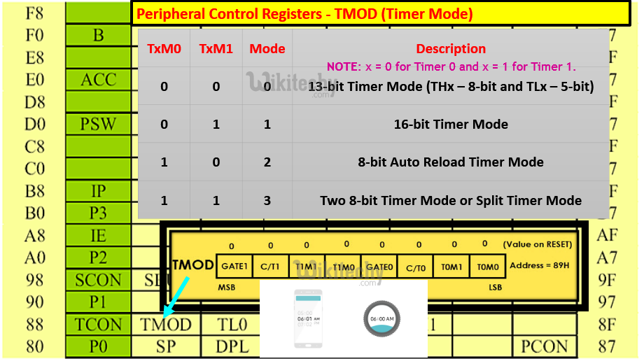
Peripheral Control Registers - TMOD (Timer Mode)
- The TMOD or Timer Mode register or SFR is used to set the Operating Modes of the Timers T0 and T1. The lower four bits are used to configure Timer0 and the higher four bits are used to configure Timer1.
Set the Operating Modes of the Timers T0 and T1
- The Gatex bit is used to operate the Timerx with respect to the INTx pin or regardless of the INTx pin.
- GATE1 = 1 ==> Timer1 is operated only if INT1 is SET.
- GATE1 = 0 ==> Timer1 is operates irrespective of INT1 pin.
- GATE0 = 1 ==> Timer0 is operated only if INT0 is SET.
- GATE0 = 0 ==> Timer0 is operates irrespective of INT0 pin.
- The C/Tx bit is used selects the source of pulses for the Timer to count.
- C/T1 = 1 ==> Timer1 counts pulses from Pin T1 (P3.5) (Counter Mode)
- C/T1 = 0 ==> Timer1 counts pulses from internal oscillator (Timer Mode)
- C/T0 = 1 ==> Timer0 counts pulses from Pin T0 (P3.4) (Counter Mode)
- C/T0 = 0 ==> Timer0 counts pulses from internal oscillator (Timer Mode)
Peripheral Control Registers - TMOD (Timer Mode)
Peripheral Control Registers - TMOD (Timer Mode) in 8051 Microcontroller
Peripheral Control Registers - IE (Interrupt Enable)
- The IE or Interrupt Enable Register is used to enable or disable individual interrupts. If a bit is SET, the corresponding interrupt is enabled and if the bit is cleared, the interrupt is disabled. The Bit7 of the IE register i.e. EA bit is used to enable or disable all the interrupts.
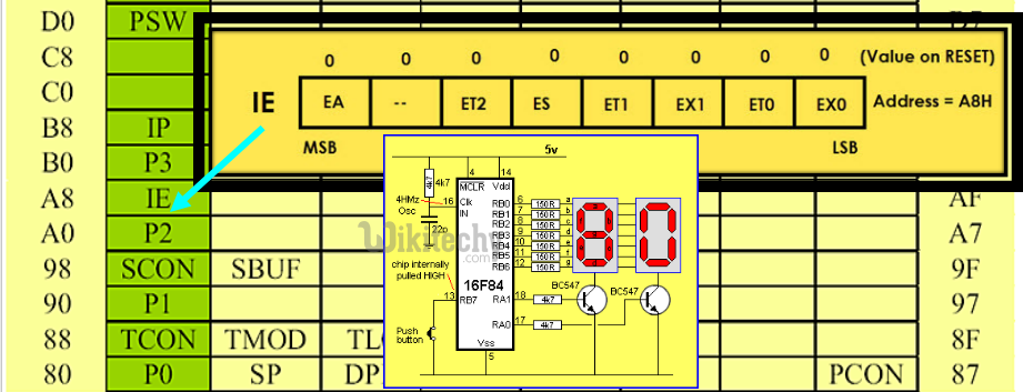
Peripheral Control Registers - IE (Interrupt Enable)
Bit is SET, the corresponding interrupt is enabled
Peripheral Control Registers - IP (Interrupt Priority)
- The IP or Interrupt Priority Register is used to set the priority of the interrupt as High or Low. If a bit is CLEARED, the corresponding interrupt is assigned low priority and if the bit is SET, the interrupt is assigned high priority.
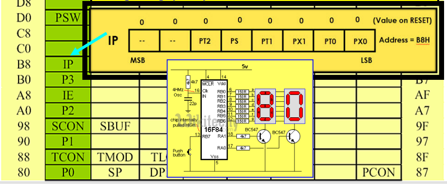
Peripheral Control Registers - IP (Interrupt Priority)
Peripheral Data Registers - SBUF (Serial Data Buffer)
- The Serial Buffer or SBUF register is used to hold the serial data while transmission or reception
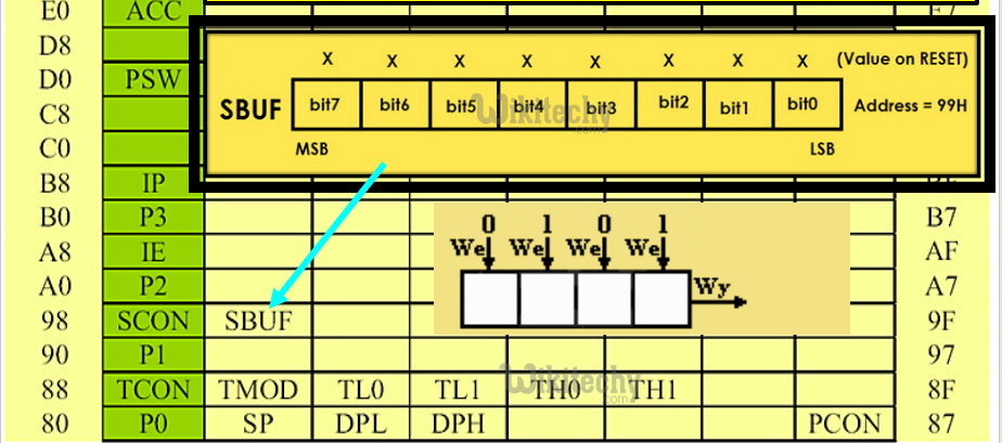
Peripheral Data Registers - SBUF (Serial Data Buffer)
Serial data processing in SBUF (Serial Data Buffer)
Peripheral Data Registers - TL0/TH0 (Timer 0 Low/High)
- The Timer 0 consists of two SFRs: TL0 and TH0. The TL0 is the lower byte and the TH0 is the higher byte and together they form a 16-bit Timer0 Register.
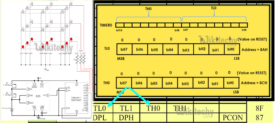
Peripheral Data Registers - TL0/TH0 (Timer 0 Low/High) in 8051 Microcontroller
Peripheral Data Registers - TL0/TH0 (Timer 0 Low/High) in Real world
Peripheral Data Registers – TL1/TH1 (Timer 1 Low/High)
- The TL1 and TH1 are the lower and higher bytes of the Timer 0.
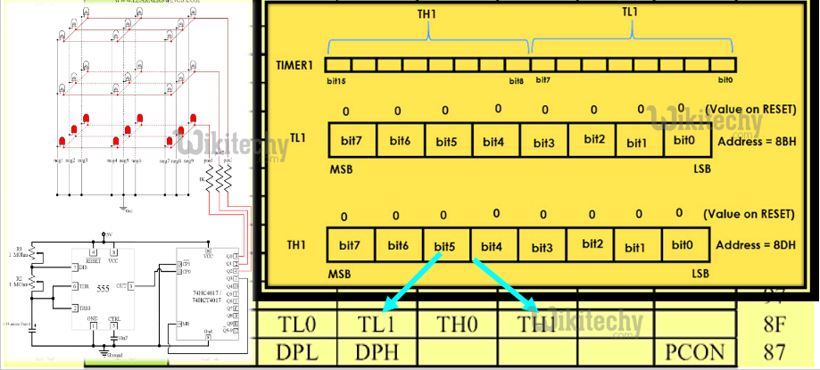
Peripheral Data Registers – TL1/TH1 (Timer 1 Low/High) in 8051 Microcontroller
Working of Peripheral Data Registers – TL1/TH1 (Timer 1 Low/High)